
Terracotta’s Flexible DRAM Interface: Buyer Takeaways
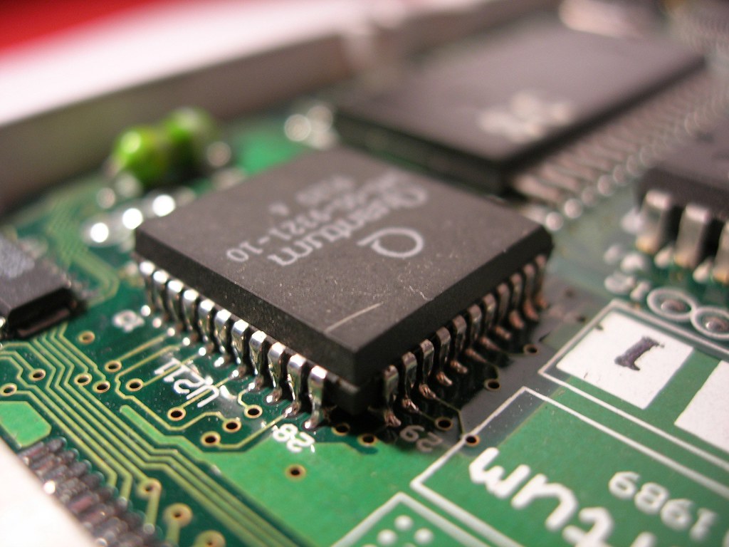
Continuity testing is still the first check in any semiconductor test flow, the step that proves the device under test is actually connected to the ATE before anyone trusts a result, as EDN’s continuity-testing primer explains. That simple fact is a useful frame for the research behind the Semiconductor Engineering headline “Programmable Memory Controller Eases Adoption of New DRAM Techniques (ETH Zürich, CISPA, NYU).” A DRAM part can pass continuity, pass a short functional screen, and still behave badly once a controller asks it to use a newer refresh, repair, security, or timing feature.
The news item is a technical paper called “Terracotta: Enabling the Adoption of New DRAM Techniques via a Flexible DRAM Interface and Memory Controller,” summarized by Semiconductor Engineering. The researchers are from ETH Zürich, CISPA, and New York University. The idea is not a faster chip by itself. It is a more programmable path between DRAM behavior and the memory controller, so new DRAM techniques can be switched on, tested, and rolled back without redesigning the whole memory subsystem every time.
Why a programmable memory controller matters beyond the lab
DRAM used to be bought mostly by density, speed grade, voltage, package, and price. That is no longer enough. Modern parts carry on-die ECC, refresh management, targeted refresh for row-hammer mitigation, post-package repair, temperature-dependent timing, and vendor-specific modes that may be visible to the controller or hidden behind JEDEC defaults. If the controller cannot expose or schedule those features, the “same” DDR5 or LPDDR5X part can act like a different device after a firmware update or a die revision.
This is where Terracotta is relevant to purchasing. A flexible controller and interface lower the friction for adopting DRAM techniques, but they also move responsibility downward into validation. Buyers will see more questions like: Which mitigation is active? Is it JEDEC-standard or vendor-specific? Does it change tREFI, tRFC, refresh overhead, latency under all-bank refresh, or read/write turnaround? Can the OEM disable it for debug? If the answer is vague, the risk lands in your incoming inspection and field returns, not in the research paper.
A recent Semiconductor Engineering paper roundup shows how wide the memory research stack has become: row-parallel processing in DRAM, high-bandwidth flash for LLM serving, 2nm backside clocking, low-contact-resistance WSe₂ transistors. For procurement, the signal is simple. Memory is not a static commodity line item anymore, even when the part number looks stable. The controller, PHY, firmware, board power integrity, and DRAM lot now form one buying decision.
Programmable Memory Controller Eases Adoption of New DRAM Techniques: the sourcing angle
For distributors and OEM buyers, “eases adoption” should translate into a tighter RFQ, not a looser one. Ask for the controller’s DRAM training log, supported DDR5/LPDDR5/HBM modes, refresh-control granularity, error counters, and whether mitigation features are locked in OTP/fuses or left in firmware. A part that can be reconfigured is useful during NPI. In production, reconfiguration can become a traceability problem if lots ship with different active features.
Use the table below as a starting checklist. Values are typical class figures, not a substitute for the JEDEC spec or the vendor datasheet.
| Memory class | Common supply / signaling | Typical data rate seen in RFQs | Package / assembly note | Buyer check tied to controller features |
|---|---|---|---|---|
| DDR5 UDIMM/RDIMM | 1.1 V VDD/VDDQ class, PMIC on DIMM | 4800-6400 MT/s | 288-pin DIMM; RDIMM adds RCD/DB | Confirm refresh mode, on-die ECC reporting, SPD hub revision, RCD firmware |
| LPDDR5/5X | Multiple low rails; roughly 1.8 V / 1.05 V / sub-1 V domains | 6400-8533 MT/s in mobile/edge quotes | BGA only; no socket rework margin | Ask for temperature derating, WCK/CK mode support, and refresh behavior at 85-105°C |
| HBM3/3E | Low-voltage stack on interposer | Above 8 Gb/s per pin class in AI accelerators | 2.5D; repair is limited after stack attach | Require known-good-stack evidence, thermal model, and repair/ECC visibility before commit |
| Legacy DDR3/DDR4 | 1.5/1.35 V or 1.2 V class | DDR3-1600 to DDR4-3200 | Long tail, higher counterfeit/pull risk | Check date codes, speed-bin remarking, and whether controller training masks marginal timing |
Two scenarios show up often in real builds. First: an industrial gateway qualifies DDR4 at -40 to 85°C, then the DRAM vendor changes die revision and refresh current rises at temperature. The system still boots at room ambient, so receiving passes it. Summer field units fail after 40-60 days. Second: an edge AI box uses LPDDR5X at 8533 MT/s, the controller team enables a mitigation mode late, and effective bandwidth drops because refresh overhead changes under sustained traffic. The memory did not become counterfeit. The configuration moved after price was approved.
This is why ATE fundamentals still matter in a research-driven story. Continuity confirms the DUT is connected; it does not prove the memory technique is configured the way your firmware expects. Good incoming test for DRAM-heavy boards should include a connector/contact check, JEDEC ID and SPD readback, a short pattern at temperature corners where practical, and a record of active controller features. For high-value builds, add serialization at the DIMM or board level and keep the training log with the lot record.
What to ask distributors before you release a PO
Keep the questions concrete. Which manufacturer, die revision, and date-code window is quoted? Is the part original franchised stock, open-market excess, or refurbished? For DRAM, refurbished usually means pulled modules or reballed components, and that may be acceptable only for non-critical repair channels. Get lot traceability before shipment, not after a failure. MOQ games are common when a speed bin tightens; if a broker can suddenly offer 50k pieces of a constrained bin at market price, treat that as a document problem until proven otherwise.
XingHuan International (icxing.com) fits best when the team needs this kind of paper trail plus practical shortage work: cross-referencing speed bins, checking date codes against OEM warranty windows, and flagging when a quote is really a different revision rather than the same memory. That matters more when a programmable controller can hide differences during a five-minute bench boot.
Lead time is the other quiet issue. If a new DRAM technique requires a controller firmware branch, your “memory lead time” includes silicon, module build, SPD/RCD firmware where relevant, validation hours, and a safe rollback image. Eight weeks for components can become fourteen weeks for a stable configuration. Buyers should write the configuration freeze into the PO: no die, firmware, SPD, RCD, or refresh-mode change without PCN-style notice and requalification evidence.
Power is part of the same conversation. AI racks are pushing designers toward higher-voltage distribution and denser conversion, as seen in EE News Europe’s report on Microchip and Navitas targeting 800V AI data-center power. Memory subsystems feel that through hotter boards, tighter VDDQ margins, and less tolerance for refresh surprises. A cheap DRAM quote that ignores airflow and rail ripple is not cheap after the first thermal throttling report.
The practical takeaway from Terracotta is not “adopt every new DRAM technique early.” It is the opposite: flexibility raises the value of disciplined configuration control. Buy the memory, the controller behavior, and the evidence package as one item.
FAQ
Q: Does a programmable memory controller reduce DRAM qualification work?
A: It can reduce redesign work, but it usually increases qualification detail. Ask for a fixed production configuration, error-counter access, and proof that refresh or mitigation settings match across date codes before you approve volume.
Q: What should receiving check first on DRAM or memory modules?
A: Start with connection and identity: visual inspection, continuity where applicable, JEDEC ID/SPD readback, date-code and lot-code match to paperwork. Then run a short temperature-corner pattern if the build is high value; room-temperature boot alone misses many marginal lots.
Q: Are open-market DRAM parts always too risky for production?
A: Not always, but the burden changes. For DDR3/DDR4 legacy stock, require traceable origin, no mixed lots without disclosure, and explicit acceptance of pull/refurb status if that is what is being sold; for current DDR5/HBM, undocumented stock is usually a poor trade.